
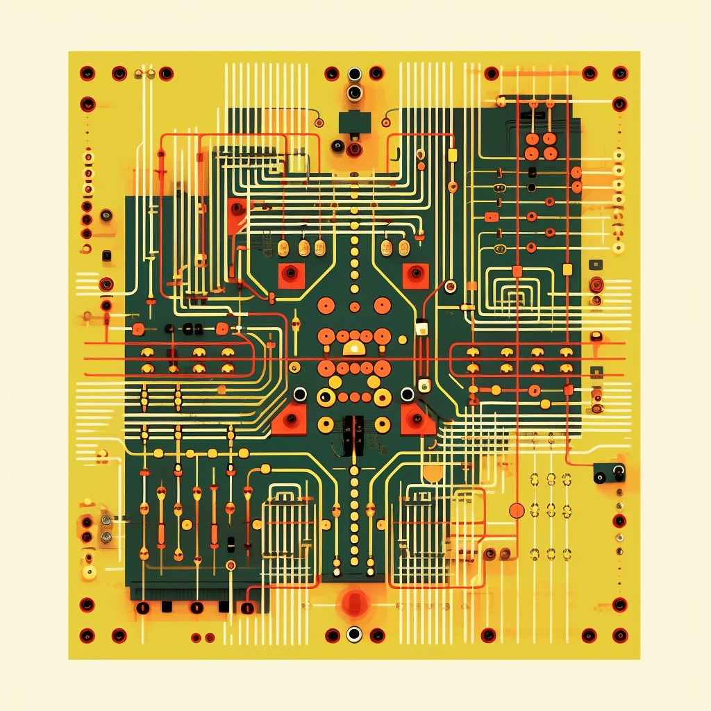
Introduction
Have you ever found yourself grappling with a non-functional printed circuit board (PCB) that holds critical importance for your operations? Do you feel helpless in the absence of its design documents, original layout, or any form of tangible support? Imagine a scenario where you are tasked with managing obsolete PCBs for which the original manufacturers no longer provide support. On top of that, you have to meet strict deadlines, maintain cost-effectiveness, and ensure the overall product quality. Sounds daunting, doesn’t it?
Fortunately, there’s a solution – PCB Reverse Engineering. This innovative process is the answer to all these predicaments. It allows you to dissect a PCB, scrutinize its components, understand their interconnections, and reproduce schematic diagrams and layout files. By employing reverse engineering, you can not only decode the workings of an existing PCB but also enhance, repair, or repurpose it to suit your specific needs.
Why is PCB Reverse Engineering Important?
Indeed, one of the most crucial benefits of PCB Reverse Engineering is that it helps to obtain the necessary manufacturing data and schematic diagrams of a given PCB.
In an ideal situation, the original manufacturer provides all the documentation needed to produce and repair a PCB, including schematic diagrams, bill of materials (BOM), and layout files. However, this is not always the case. Sometimes, these crucial pieces of information are lost, not provided, or are outdated due to various reasons such as obsolescence, discontinuation of the product, or business closures.
In such scenarios, PCB Reverse Engineering becomes a lifesaver. It is a systematic process that involves deconstructing the PCB, identifying and studying its components, understanding their interconnections, and using this information to recreate the schematic diagram and production data.
The extracted schematic diagram serves as a ‘map’ of the PCB, revealing how different components are connected and interact with each other. It provides valuable insights into the PCB’s design and functioning, which is critical for troubleshooting, repairs, modifications, and enhancements.
The manufacturing data derived through reverse engineering ensures that you can replicate the PCB without relying on the original manufacturer. It includes the exact details of components used, their placement and orientation on the board, and other important information required for production.
Thus, PCB Reverse Engineering not only helps to keep your operations running smoothly but also empowers you to take control of your PCB needs. It reduces dependency on the original manufacturers and allows for flexibility in maintaining and enhancing the product according to your requirements.
What is PCB Reverse Engineering?
PCB Reverse Engineering is a comprehensive process that involves understanding, analyzing, and duplicating an existing printed circuit board (PCB), especially when original design records or data are either unavailable or outdated.
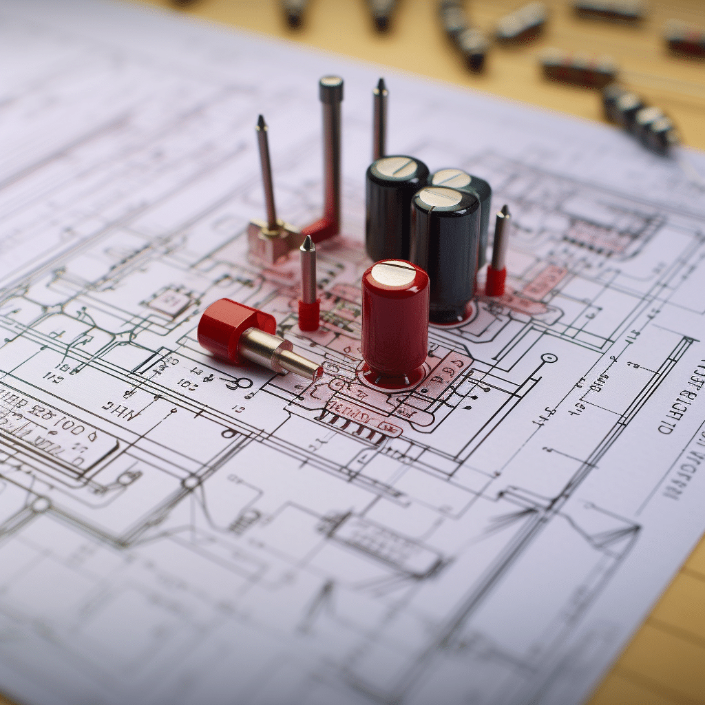
The fundamental premise of PCB reverse engineering lies in the careful deconstruction of the board. This process starts with the identification and documentation of the board’s components, including resistors, capacitors, inductors, integrated circuits (ICs), and more.
The next step involves understanding the interconnections between these components, which essentially forms the circuit. This is achieved by tracing the circuit paths on the PCB. Specialized equipment, such as multimeters, may be used in this step to determine the links between components and their orientation on the board.
Once the components and their connections are fully identified, the information is used to recreate the schematic diagram of the PCB. The schematic diagram is a graphical representation of the components and their interconnections, forming a ‘blueprint’ of the circuit.
The final part of reverse engineering involves reproducing the layout files, which contain details such as the size and shape of the PCB, the placement of components, the paths of the circuit traces, and other essential production information. This data is critical for manufacturing the PCB.
Thus, PCB reverse engineering is a meticulous process of deconstruction, analysis, and recreation that allows engineers to obtain invaluable information about a PCB’s design and function when the original data is lost or unavailable. This knowledge can then be used for a variety of applications, including troubleshooting, component replacement, design improvement, and even creating entirely new, innovative products.
The Process of PCB Reverse Engineering

The process of PCB reverse engineering involves a systematic approach to decode the design and functionality of a given PCB. Here’s a detailed explanation of the process, broken down into three essential steps.
Understanding the Original Design
The first step in the process involves thoroughly examining the original PCB. This step can be compared to an archeological excavation where each component and connection is carefully analyzed. The purpose is to understand the complete structure of the PCB and to make a list of components used on the board, including resistors, capacitors, integrated circuits (ICs), connectors, and more.
The reverse engineering team will inspect the board visually, and then with the help of specialized equipment, including multimeters, oscilloscopes, and sometimes even X-ray imaging machines to reveal the layers beneath the surface. The team will take detailed notes, make sketches, and capture high-resolution photographs to document the PCB’s layout.
Rebuilding the Schematic Diagram
Once the team has a clear understanding of the PCB’s design, the next step is to rebuild the schematic diagram. This diagram represents all the components of the PCB and the interconnections between them.
The engineers start by tracing the electrical paths or tracks on the PCB and noting down their findings. This step requires a good understanding of electronic components and circuit design, as well as meticulous attention to detail.
The final schematic diagram will be a graphical representation of the PCB, where each symbol represents a specific component, and lines represent the connections between them.
Replicating the PCB Layout
With a fully-fledged schematic diagram at hand, the final step is to recreate the PCB layout. The layout includes the precise locations of components on the PCB, the routing of the electrical tracks, and other mechanical details like the size and shape of the board, drill holes, etc.
The engineers will use specialized PCB design software to create a digital version of the layout. This digital model will contain all the information necessary to manufacture the PCB, including the Bill of Materials (BOM), Gerber files, and other manufacturing data.
In summary, PCB Reverse Engineering is a labor-intensive, highly detailed process that requires specialized skills and equipment. But, it is an invaluable tool for understanding, replicating, and improving upon existing PCB designs, especially when original documentation is not available.
Challenges in PCB Reverse Engineering
While PCB Reverse Engineering offers a multitude of benefits, it’s not without its challenges. Here are some of the key difficulties often encountered during this process.
Intellectual Property Rights
One of the primary concerns in reverse engineering is the potential violation of intellectual property rights. Reverse engineering a PCB may lead to unauthorized duplication of patented technology, which can result in serious legal consequences. It’s crucial for any organization undertaking reverse engineering to understand and respect the existing laws and regulations regarding intellectual property rights.
Chip Decryption
The soul of a PCBA (Printed Circuit Board Assembly) resides within the firmware embedded in its chips. Without this software, the PCBA would be unable to function. Therefore, one of the most significant challenges in PCB Reverse Engineering involves decrypting the chip or extracting its firmware.
Firmware extraction is a sophisticated process that involves reading the firmware data from the chip, decoding it, and understanding its functionality. This is usually done using specialized tools and equipment. However, modern chips often come equipped with security features to prevent unauthorized access, making this task extremely challenging. In some cases, the firmware may be encrypted, further complicating the decryption process.
However, if successful, chip decryption provides access to the firmware’s source code. This code can reveal how the PCB functions on a software level, allowing for further insights into its operation, potential improvements, and the ability to replicate the PCB’s functionality in a new design.
Technological Complexity
As technology continues to evolve, so does the complexity of PCBs. Modern PCBs often consist of multiple layers and can contain hundreds, or even thousands, of components in a very compact area. Tracing connections, identifying components, and reproducing the layout of these complex boards can be extremely challenging. It requires highly skilled engineers, specialized equipment, and a lot of patience.
Furthermore, some components may be custom-made or obsolete, making them difficult to identify or source. Some PCBs may also include programmable components, such as microcontrollers, for which firmware data might be needed, adding another layer of complexity to the reverse engineering process.
Assessing Time and Cost in PCB Reverse Engineering
The time and cost involved in PCB Reverse Engineering often depend on the complexity of the PCB and the specific goals of the project. While the process can be lengthy and may require a significant investment, it is essential to consider the potential long-term benefits.
For PCBs that are discontinued or prohibitively expensive to procure, reverse engineering could serve as a cost-effective alternative. While there are upfront costs, the ability to replicate the original PCB can lead to substantial cost savings in the long run. This is particularly true for systems that rely on a specific PCB, where redesigning the system to accommodate a different PCB could be even more costly.
The timeframe for a reverse engineering project can vary widely depending on the PCB’s complexity. A simple, single-layer PCB could be reverse-engineered in a relatively short period, while a complex, multi-layer PCB with hundreds of components and firmware may take significantly longer.
It’s also important to consider the time associated with potential roadblocks, such as challenges in chip decryption. Modern chips often have security features designed to prevent unauthorized access, which can add to the time required for the reverse engineering process.
In conclusion, while PCB Reverse Engineering does require an investment of time and resources, its potential benefits often make it a worthwhile endeavor. By allowing for the replication of hard-to-source or expensive PCBs, reverse engineering can be a crucial tool in maintaining and extending the lifespan of electronic systems.
The Role of PCB Reverse Engineering in Improving Design and Manufacturing
PCB Reverse Engineering plays a significant role in enhancing both design and manufacturing processes within the electronics industry. This is achieved through various means:
Learning from Existing Designs
Reverse engineering allows engineers to learn from existing PCB designs, including those created by competitors. By understanding the design choices and trade-offs made by others, engineers can gain insights into effective design strategies and potentially discover innovative solutions for their own designs. This kind of benchmarking can significantly enhance a company’s design capabilities and lead to more competitive products.
Replicating Successful Designs
At times, companies might need to replicate successful PCB designs, particularly when original components are discontinued or hard to source. Through reverse engineering, these designs can be replicated accurately, maintaining the functionality and performance of the original systems. This allows the continuation of production without significant downtime or the need for extensive system redesigns.
Improving Manufacturing Processes
By reverse engineering a PCB, engineers can gain a deeper understanding of its manufacturing requirements. This can lead to improved manufacturing processes, as potential bottlenecks or issues can be identified and resolved. In turn, this can lead to increased manufacturing efficiency and better product quality.
Facilitating Customization
PCB Reverse Engineering can also facilitate customization. Once a PCB has been reverse-engineered, changes can be made to the design to meet specific requirements. This allows for the customization of electronic systems, improving their fit with specific applications or environments.
In conclusion, PCB Reverse Engineering serves as a vital tool in the electronics industry, enabling continuous improvement in design and manufacturing processes. By understanding and replicating successful designs, enhancing manufacturing processes, and facilitating customization, reverse engineering contributes to the advancement of the industry as a whole.
How Rowsum Delivers Quality in PCB Reverse Engineering
Rowsum, as a leader in PCB manufacturing and services, places a strong emphasis on quality in all its processes, and PCB Reverse Engineering is no exception. Here’s how Rowsum ensures quality in its reverse engineering services:
- Experienced Engineering Team
Rowsum has a team of highly skilled and experienced engineers with expertise in PCB Reverse Engineering. Our team understands the complexities and intricacies of PCBs and can efficiently decipher and replicate designs with a high degree of accuracy. This commitment to excellence and our team’s expert skills ensure that the reverse-engineered PCBs maintain the same functionality and reliability as the originals.
- State-of-the-art Equipment
At Rowsum, we use advanced equipment and tools for our reverse engineering processes. This includes high-precision 3D scanners and cutting-edge design software, which allow us to recreate precise and accurate PCB designs. The use of such advanced tools reduces the likelihood of errors and ensures high-quality outputs.
- Customer-Centric Approach
At Rowsum, we prioritize our customers’ needs. Our reverse engineering process is tailored to suit the specific requirements of each customer. Whether it’s replicating a discontinued PCB or making modifications to an existing design, we ensure that our services align with our client’s business goals.
- Quality Assurance
To ensure the quality of our reverse-engineered PCBs, Rowsum has stringent quality control processes in place. These include rigorous testing and inspection procedures, which are carried out to verify the functionality and reliability of our products.
- Transparent Communication and Project Assessment
Unlike many competitors in the field, Rowsum doesn’t blindly promise successful reverse engineering outcomes. We understand that not all PCBs can be reverse engineered easily, especially when chip decryption is involved.
Therefore, we prioritize clear, upfront communication with our clients. Before the start of a project, we have detailed discussions with clients about their specific requirements, evaluate the PCB they want to reverse engineer, and assess the project’s success likelihood. This process may involve confirming the details of the PCB, the components used, the complexity of the design, and the feasibility of chip decryption.
By being transparent about the potential challenges and the success likelihood, we ensure that clients can make informed decisions. This approach not only avoids unnecessary disappointments and wastes of time but also builds trust with our clients.
We take pride in offering transparent project assessment, saving our clients from potential disappointments and time wastage. Your need for reliable, accurate, and cost-effective PCB Reverse Engineering services is our top priority. Rowsum is dedicated to providing solutions that precisely align with your business goals, making us an excellent partner for your PCB Reverse Engineering needs.
FAQs
1. Why is chip decryption necessary in PCB Reverse Engineering?
Chip decryption is often a crucial step in PCB Reverse Engineering as the chip contains the program that makes the PCBA operational. Without decrypting the chip, the reverse engineered PCB wouldn’t function as the original did, making this process vital.
2. Why are the upfront costs of PCB Reverse Engineering often high?
The upfront costs of PCB Reverse Engineering can be significant due to the specialized tools, equipment, and skilled professionals needed for the process. Moreover, complex PCBs or those with encrypted chips may require more time and resources to decipher, adding to the cost.
3. What makes Rowsum an ideal choice for PCB Reverse Engineering?
Rowsum has an experienced engineering team and utilizes state-of-the-art equipment for PCB Reverse Engineering. We follow ethical practices, ensure transparency in project assessments, and adopt a customer-centric approach to deliver high-quality and cost-effective solutions.
4. Can PCB Reverse Engineering help if original components of my PCB are discontinued or hard to source?
Absolutely. PCB Reverse Engineering can help replicate successful designs when original components are discontinued or hard to source. This allows production to continue without significant downtime or extensive system redesigns.
Certainly, here’s the revised fifth question:
5. What’s the difference between PCB Reverse Engineering and PCB Development?
PCB Reverse Engineering and PCB Development are fundamentally different processes. PCB Reverse Engineering involves deconstructing a finished PCB to understand its design and functionality. It aims at recreating the schematic diagram, bill of materials (BOM), and design files from an existing physical PCB.
On the other hand, PCB Development is the process of designing and manufacturing a PCB from scratch. It starts with conceptualizing the electronic circuit, creating the schematic diagram, designing the PCB layout, and finally manufacturing the PCB.
While PCB Development focuses on creating a new product, PCB Reverse Engineering concentrates on understanding and replicating an already existing one.