Introduction to PCB Basics
Welcome to the fascinating world of Printed Circuit Boards (PCBs)! In this article, we’ll explore the basics of PCBs, including their components, how they work, materials used, design and manufacturing processes, and much more. So, let’s dive in and discover the essential elements of this incredible technology!
What is a Printed Circuit Board (PCB)?
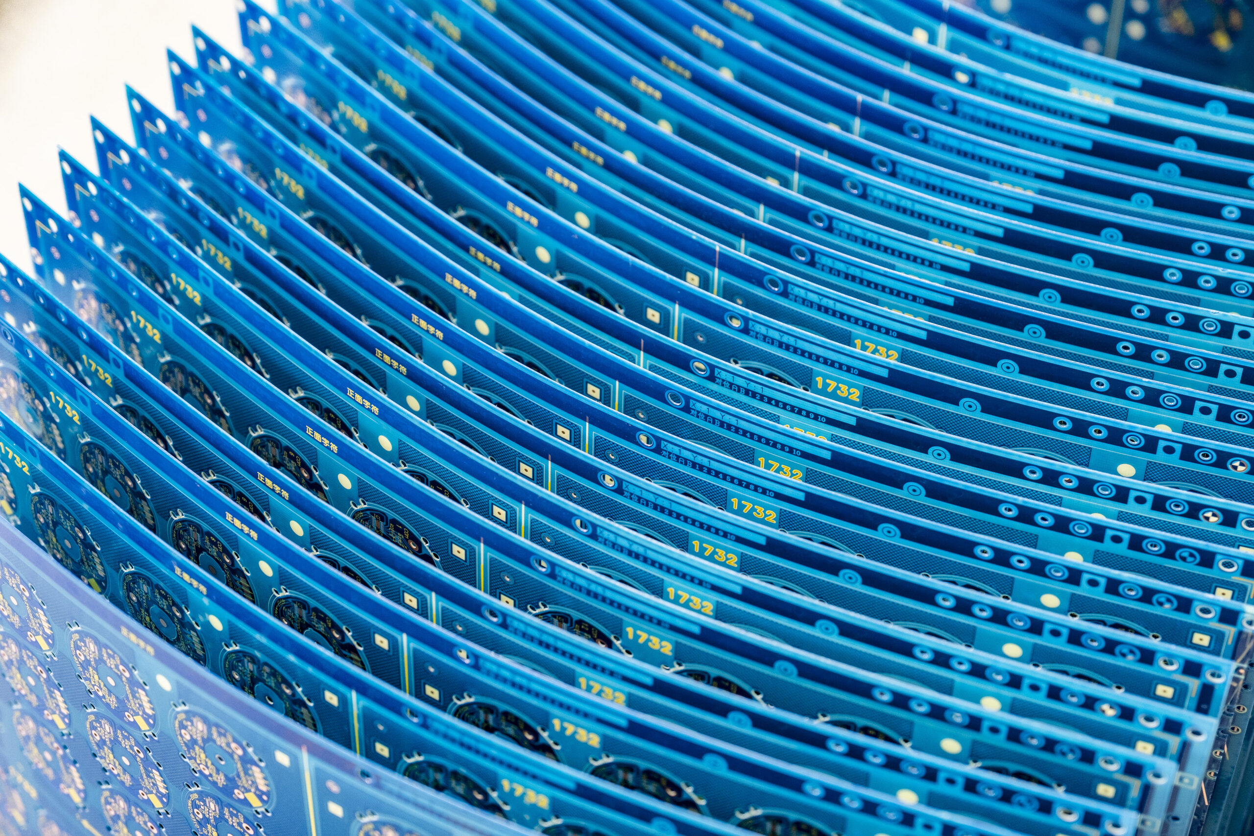
A Printed Circuit Board (PCB) is the backbone of virtually all modern electronic devices. It provides a platform for connecting and supporting electronic components, such as resistors, capacitors, and integrated circuits. By mechanically supporting and electrically connecting these components, PCBs enable complex electronic systems to function efficiently.
Components of a PCB
A typical PCB consists of various layers and components, including:
- Substrate: The base material, usually made of fiberglass (FR4) or other insulating materials, that provides mechanical support to the board.
- Copper layers: Thin layers of conductive copper that form the circuits and connections between electronic components.
- Solder mask: A protective layer applied over the copper, which prevents short circuits and protects the board from environmental factors.
- Silkscreen: A layer of ink printed on the PCB that provides labels, symbols, and other information for easy identification and assembly.
Types of PCBs
PCBs come in various forms, including:
- Single-sided PCBs: Contain only one layer of copper, suitable for simple electronic devices.
- Double-sided PCBs: Have copper layers on both sides, allowing for more complex circuits and increased component density.
- Multi-layer PCBs: Feature multiple layers of copper, separated by insulating materials, enabling high-density circuits and advanced functionality.
How Do PCBs Work?
Circuit Design
The functionality of a PCB depends on the arrangement of its circuits, which are designed to achieve a specific purpose. These circuits are made up of traces (copper pathways) that connect different electronic components, enabling the flow of electrical current and signals between them. Circuit design involves creating an efficient layout that minimizes signal interference, power consumption, and overall board size while maximizing performance and reliability.
Electronic Components
Various electronic components are mounted on a PCB to perform specific functions, such as processing data, amplifying signals, or storing information. These components can be either through-hole (inserted into holes drilled in the PCB) or surface-mount (attached directly to the surface of the PCB). The choice between these two mounting techniques depends on factors like component size, manufacturing complexity, and overall performance requirements.
PCB Materials
Substrate
The substrate, or base material, provides mechanical support and electrical insulation for the PCB. The most commonly used substrate is fiberglass-reinforced epoxy (FR4), known for its excellent insulating properties, strength, and durability. Other substrate materials include polyimide, ceramic, and metal-core PCBs, each with its own unique advantages and applications.
Copper Layers
Copper layers form the circuits and connections on a PCB. The thickness of these layers is typically measured in ounces per square foot (oz/ft²), with common thicknesses ranging from 0.5 oz/ft² to 2 oz/ft². Thicker copper layers are used for higher current applications or when increased thermal dissipation is required.
Solder Mask
The solder mask is a protective layer applied over the copper to prevent short circuits and protect the board from environmental factors such as moisture, dust, and chemicals. It also provides insulation between conductive traces and ensures that solder only adheres to designated areas during assembly. Solder masks are usually made of epoxy-based materials and come in various colors, with green being the most common.
Silkscreen
Silkscreen is a layer of ink printed on the PCB, providing labels, symbols, and other information for easy identification and assembly. It can include component designations, polarity indicators, and company logos. Silkscreen is typically white, but other colors can be used depending on the board’s design requirements.
PCB Design Process
Schematic Design
The first step in the PCB design process is creating a schematic, which is a visual representation of the electronic circuit. It shows the connections between components and is used as a reference throughout the design process. Designers use schematic capture software to create and edit schematics, ensuring that all connections and components are accounted for.
Layout Design
Once the schematic is complete, the layout design begins. This involves arranging the components on the PCB, routing the copper traces to connect them, and defining the board’s dimensions and layers. Designers use electronic design automation (EDA) software, also known as computer-aided design (CAD) software, to create and optimize the layout.
Gerber File Generation
After the layout design is finalized, the designer generates a set of files known as Gerber files. These files contain detailed information about the PCB’s layers, dimensions, and component placement, serving as a blueprint for the manufacturing process.
PCB Manufacturing Process
Substrate Preparation
The PCB manufacturing process begins with the preparation of the substrate material. For FR4 substrates, this involves cutting the fiberglass sheets to the required size and laminating them with a layer of copper on one or both sides.
Copper Layer Deposition
For multi-layer PCBs, additional copper layers are added by a process called electroplating. This involves depositing a thin layer of copper onto the substrate using an electrical current.
Etching
Etching is the process of removing unwanted copper from the PCB, leaving only the desired traces and connections. This is typically done using a chemical etchant that dissolves the exposed copper while leaving the protected copper (covered by a temporary mask) intact. The mask is then removed, revealing the final copper circuit pattern.
Solder Mask Application
Next, the solder mask is applied to the PCB to protect the copper traces and prevent short circuits. This involves coating the board with a thin layer of solder mask material, which is then cured using ultraviolet (UV) light. The solder mask openings are precisely aligned with the copper pads, ensuring accurate component placement during assembly.
Silkscreen Printing
The silkscreen layer is printed onto the PCB, providing component designations, symbols, and other relevant information. This process involves either screen printing or inkjet printing the desired text and graphics onto the board.
Drilling and Routing
Holes are drilled into the PCB to accommodate through-hole components and to create vias (electrical connections between layers). High-speed, computer-controlled drilling machines are used to ensure accurate hole placement and size. After drilling, the PCB is routed to its final shape, with any necessary cutouts and slots created.
Surface Finishing
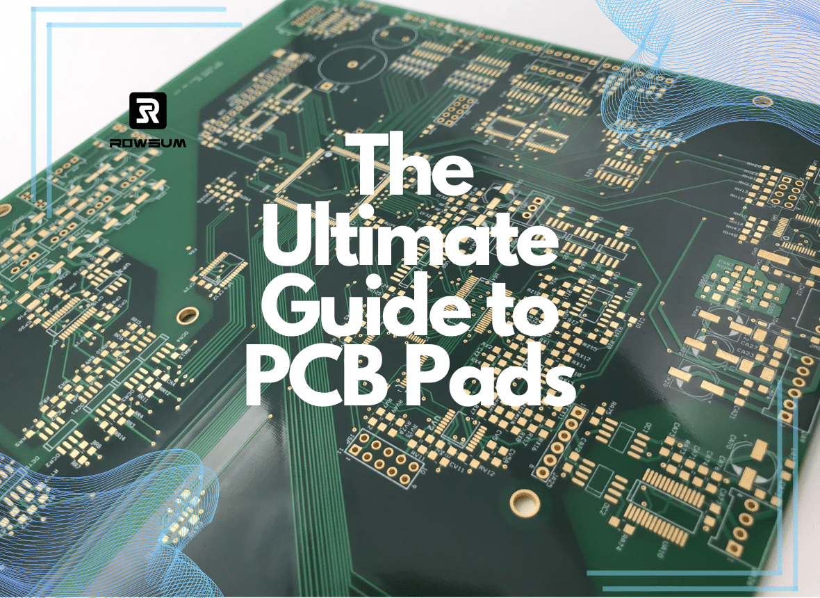
The final step in the PCB manufacturing process is surface finishing, which involves applying a protective coating to the exposed copper pads. Common surface finishes include Hot Air Solder Leveling (HASL), Electroless Nickel Immersion Gold (ENIG), and Immersion Silver. Each finish type offers unique advantages in terms of solderability, corrosion resistance, and cost.
PCB Assembly
PCB assembly involves attaching electronic components to the PCB, either through-hole or surface-mount. This process can be done manually, but automated assembly machines are commonly used for faster and more accurate component placement. After assembly, soldering is performed to create strong electrical connections between the components and the board.
PCB Testing and Inspection
Once the PCB is assembled, it undergoes testing and inspection to ensure proper functionality and adherence to quality standards. Common testing methods include visual inspection, automated optical inspection (AOI), X-ray inspection, and functional testing. These tests help identify any defects, such as missing or misplaced components, soldering issues, or short circuits.
Common PCB Issues and Solutions
Some common PCB issues include:
- Solder bridges: Occur when solder flows between adjacent pads, creating a short circuit. Solution: Careful soldering techniques and proper solder mask application.
- Copper corrosion: Caused by exposure to moisture, chemicals, or other environmental factors. Solution: Use of protective surface finishes and proper storage practices.
- Thermal stress: Occurs when components or traces experience excessive heat, leading to performance issues or failures. Solution: Proper component placement, heat sinks, and thermal vias.
Future Trends in PCB Technology
As electronics continue to evolve, PCB technology is also advancing to meet new demands. Some future trends include:
- Flexible PCBs: Made from flexible materials, allowing for innovative form factors and applications.
- Embedded components: Integrating passive components directly into the PCB substrate, reducing size and improving performance.
- High-density interconnect (HDI) technology: Allows for smaller, more complex PCBs with increased component density and improved signal integrity.
Conclusion
Understanding the basics of PCBs is essential for anyone involved in electronics, from hobbyists to professionals. From design and materials to manufacturing and testing, each aspect of the PCB process plays a critical role in creating reliable, high-performance electronic devices. As technology advances, the importance of PCBs in our daily lives is only set to increase, making it an exciting field to explore and master.
FAQs
What is the primary purpose of a PCB? The primary purpose of a PCB is to provide a platform for connecting and supporting electronic components, enabling complex electronic systems to function efficiently.
What are the main types of PCBs? The main types of PCBs include single-sided, double-sided, and multi-layer PCBs. Single-sided PCBs have one copper layer, double-sided PCBs have copper layers on both sides, and multi-layer PCBs have multiple layers of copper separated by insulating materials.
Why is a solder mask important in PCB design? A solder mask is important because it protects the copper traces from short circuits, environmental factors (e.g., moisture, dust, and chemicals), and provides insulation between conductive traces. It also ensures that solder only adheres to designated areas during assembly.
What are some common materials used in PCBs? Common materials used in PCBs include fiberglass-reinforced epoxy (FR4) for the substrate, copper for the circuit layers, epoxy-based materials for the solder mask, and ink for the silkscreen layer.
How do PCB designers ensure the functionality and reliability of their boards? PCB designers ensure functionality and reliability through careful circuit design, component selection, and layout optimization. They also follow best practices in manufacturing, testing, and inspection to identify and resolve any potential issues.

