Ever felt lost hearing terms like ‘FR4,’ ‘Gerber files,’ or ‘AQL’ in a PCB discussion? Picture this: you’re in a meeting with suppliers, and they’re talking about ‘HDI,’ ‘AOI,’ and ‘RoHS compliance.’ You nod, but you’re not really following. You’re not alone. The PCB world is full of terms that can be confusing.
This guide is here to change that. We’ve put in the work to compile the most complete list of PCB terminology you’ll find. Whether you’re an engineer, a procurement manager, or just curious, this guide is your key to understanding PCBs better.
Manufacturing and Assembly Terms
Materials
FR4 (Flame Retardant 4)
This is the most commonly used material for the substrate in PCBs. It’s known for its durability and flame-resistant properties.
Copper
This is the conductive material used for traces, pads, and planes on the PCB. It comes in various thicknesses, often measured in ounces per square foot.
Solder Mask
This is the layer that covers the copper traces, providing insulation and protection. It’s usually green but can come in other colors.
Silkscreen
This is the layer where labels and symbols are printed to indicate component placement and other information.
Prepreg
This is a fibrous material impregnated with resin, used to bond layers together in multilayer PCBs.
Phenolic Resin
This is a less expensive alternative to FR4, often used in consumer electronics. However, it’s less durable and not flame-resistant.
Polyimide
This material is used for flexible PCBs. It’s known for its ability to withstand high temperatures.
High-Frequency Materials
These are specialized materials used in high-frequency applications, like Rogers or Teflon.
Lead-Free Solder
This is used in RoHS-compliant PCBs to attach components without using lead, which is harmful to the environment.
Thermal Paste
This is used to improve the thermal contact between heat-producing components and heat sinks.
Aluminum
Used primarily for its heat-dissipating capabilities, aluminum boards are commonly found in LED and power supply applications.
Glass-Reinforced Epoxy
This is a composite material made of glass fiber cloth and epoxy resin. It’s commonly used in PCBs for its excellent strength, low moisture absorption, and superior electrical properties.
Ceramic
Known for its high-temperature resistance and excellent electrical insulation, ceramic boards are often used in extremely high-temperature environments.
PTFE (Polytetrafluoroethylene)
Commonly known by its brand name Teflon, PTFE is used in high-frequency applications due to its low dielectric constant.
Aramid
This material is known for its strength and is used in applications where mechanical stability is crucial.
Gold
Used in some specialized applications for its excellent conductivity, gold is often found in high-reliability boards.
Carbon Ink
Used to create a conductive surface for keypads, touch screens, and other input devices.
Epoxy Resin
Often used in combination with other materials like FR4 to provide structural integrity to the board.
Stainless Steel
Sometimes used as a stiffener in flexible PCBs to provide mechanical support.
Fabrication Processes
Etching
This is the process of removing unwanted copper from the board to form the traces and pads. Chemical solutions are often used for this purpose.
Drilling
Holes are drilled into the board to allow for the mounting of through-hole components. The holes are usually then plated with copper.
Plating
This involves adding a layer of copper to the drilled holes to create a conductive channel between the board layers.
Lamination
Multiple layers of material are fused together under heat and pressure to form a multilayer board.
ALIVH
A specialized technology used for constructing multilayer Build-Up (BUM) PCBs, allowing for internal vias between any layers.
Backdrilling
A technique used to remove excess copper from the plated-through holes to improve signal integrity.
Circuit Pattern
The layout of copper traces that form the electrical pathways on a PCB.
Conductor Spacing
The minimum allowable distance between adjacent copper traces to prevent electrical interference.
Copper Weight
A measure of the thickness of the copper layers on a PCB, usually expressed in ounces per square foot.
Blind Via
A via that connects an outer layer to one or more inner layers but does not go through the entire board.
Buried Via
A via that connects two or more inner layers and is not visible from the outer layers.
Differential Pair
Two closely spaced traces that carry complementary signals, reducing electromagnetic interference.
Annular Ring
The copper area that remains around a drilled hole, critical for ensuring strong solder connections.
Aspect Ratio
The ratio of the PCB’s thickness to the diameter of its smallest via, an important factor in PCB manufacturing.
Anti-Solder Ball
A technique commonly employed in Surface Mount Technology (SMT) lines to prevent the formation of solder balls during reflow.
Photolithography
This is a process used to transfer geometric shapes on a mask to the surface of a substrate. It’s a crucial part of the etching process in PCB manufacturing, allowing for the precise patterning of the copper layer.
Solder Mask Application
A layer of solder mask is applied over the copper to insulate and protect it, as well as to prevent solder bridges.
Silkscreen Printing
Symbols, letters, and numbers are printed onto the board to indicate component locations and other information.
Surface Finish
A surface finish like HASL or ENIG is applied to protect the copper and improve its solderability.
Electrical Testing
The board is tested for electrical continuity to ensure that there are no open or short circuits.
Scoring and Profiling
The board is cut into its final shape, and any necessary scoring is added to facilitate later separation of individual boards from a panel.
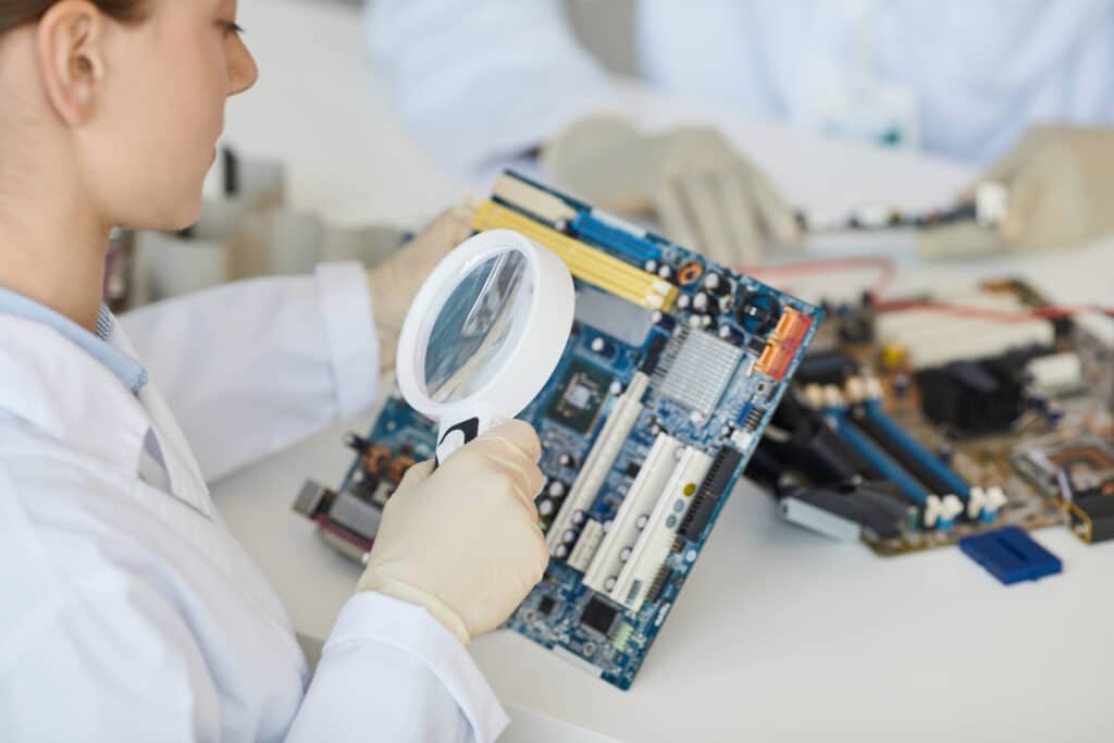
Quality Control
The board undergoes various inspections, including visual and automated checks, to ensure it meets quality standards.
Assembly Techniques
Assembly
The sequential process involving the placement of electronic components and accessories onto a PCB.
Component Placement
Before soldering, components are placed on the board according to the design. This can be done manually or by automated machines.
Surface-Mount Technology (SMT)
This is the most common method of attaching components to a PCB. It involves placing components directly onto the surface of the board.
Through-Hole Technology (THT)
In this method, components with wire leads are inserted into holes drilled into the PCB. This is an older technique but is still used for components that need to withstand mechanical stress.
Ball Grid Array (BGA)
A surface-mount packaging technology where the pins are arranged in a grid pattern on the underside of the package.
Bed of Nails
A testing method that uses a custom fixture with spring-loaded pins to make electrical contact with the test points on a PCB.
Controlled Impedance
The practice of designing a PCB to ensure that signal traces maintain a consistent impedance, improving signal integrity.
Daisy Chain
A wiring scheme where multiple devices are connected in series, one following the other.
Mixed Assembly
This involves using both SMT and THT techniques on the same board, often for specialized applications.
Reflow Soldering
This is a process where solder paste is melted to permanently attach components to the board. It’s commonly used in SMT assembly.
Selective Soldering
This is a soldering process where only specific components are soldered, avoiding areas that are sensitive to heat. It’s particularly useful for boards that have both through-hole and surface-mount components.
Wave Soldering
This is another soldering method, mainly used for THT components. The board passes over a wave of molten solder to attach the components.
Hand Soldering
This is the manual process of soldering components onto a board, often used for prototypes or small-scale production.
Automated Assembly
Robotic arms and other automated machinery are used to place and solder components, ideal for large-scale manufacturing.
Functional Testing
Beyond just electrical continuity, the board may also be tested to ensure that it performs its intended function correctly.
Conformal Coating
A protective chemical coating is applied to the board to protect it from environmental factors like moisture and dust.
Quality Control
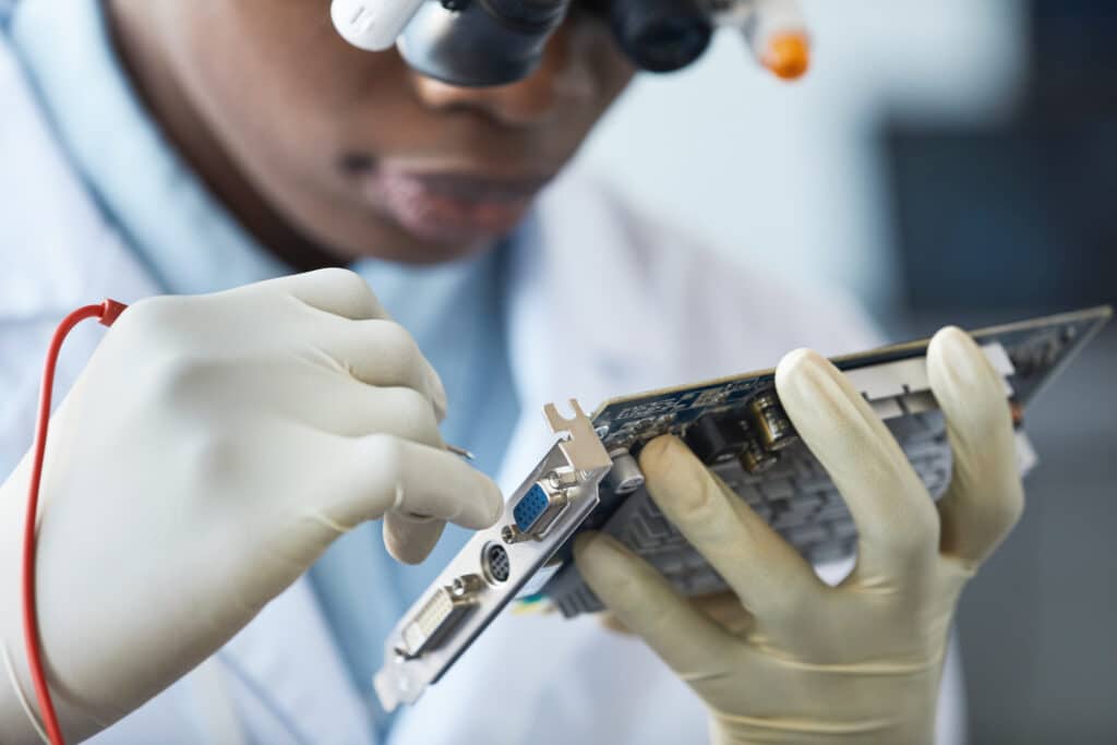
Automated Optical Inspection (AOI)
Automated Optical Inspection, a quality control method used to identify potential soldering issues in multilayer PCBs.
X-ray Inspection
This advanced inspection method uses X-rays to view the internal features of a PCB. It’s especially useful for checking the quality of solder joints that are not visible to the naked eye, such as those in Ball Grid Arrays (BGAs).
In-Circuit Test (ICT)
This involves testing the electrical performance of a PCB to ensure that all components are functioning as intended.
Functional Test
This is a type of quality control test where the PCB is tested under conditions that mimic its intended operation.
Environmental Stress Testing
This involves subjecting the PCB to various environmental conditions like temperature and humidity to ensure its reliability.
Acceptable Quality Level (AQL)
Acceptable Quality Level, a standard used to assess the quality of production practices by assembly manufacturers.
First Article Inspection (FAI)
This is an initial sample inspection to ensure that all processes, documentation, and tooling are capable of producing parts that meet specifications.
Statistical Process Control (SPC)
This involves using statistical methods to monitor and control the quality of the manufacturing process.
Failure Mode and Effects Analysis (FMEA)
This is a systematic approach to identifying potential failure modes and determining their impact on the system.
Quality Assurance (QA)
This is the process of verifying whether a product meets required specifications and customer expectations.
Quality Control Charts
These are graphs used to study how a process changes over time, aiding in understanding and improving process efficiency.
Array
A panel containing multiple identical PCBs, often used to improve manufacturing efficiency.
Six Sigma
This is a set of techniques and tools for process improvement. It seeks to improve the quality of process outputs by identifying and removing the causes of defects and minimizing variability in manufacturing and business processes.
Surface Finishes
Hot Air Solder Leveling (HASL)
This is the most common and least expensive type of finish, where molten solder is used to coat the board.
Lead-Free HASL
Similar to HASL but uses a lead-free solder alloy, making it RoHS compliant.
Electroless Nickel Immersion Gold (ENIG)
This finish provides a flat surface and excellent solderability, making it ideal for surface-mount applications.
Immersion Silver
This is a simple and cost-effective finish that offers good solderability but is sensitive to handling and environment.
Immersion Tin
This finish is flat and excellent for fine-pitch components but is not ideal for multiple reflow/assembly processes.
Organic Solderability Preservatives (OSP)
This is an organic finish that provides a very flat surface but has a limited shelf life.
Hard Gold
This finish is used for edge connectors because of its durability but is more expensive.
Soft Gold
This is used for wire bonding and offers excellent surface flatness but is also more expensive.
Electroplated Nickel/Gold
This is a very robust finish used in high-reliability applications but is the most expensive option.
Selective Finishes
These are custom finishes that are used in specialized applications, often a combination of the above finishes.
Immersion Gold over Nickel
This is a two-layer metallic coating with a layer of nickel underneath the gold. It provides excellent surface planarity, making it ideal for fine-pitch and BGA components.
Packaging and Shipping
Anti-Static Bags
These are used to prevent static electricity from damaging the PCBs. They are usually the first layer of packaging.
Bubble Wrap
This provides additional protection against mechanical damage during shipping.
Cardboard Boxes
These are the outer layer of packaging and are used for their durability and ease of handling.
Vacuum Sealing
Some sensitive components may require vacuum sealing to prevent moisture ingress.
Palletizing
For large orders, PCBs may be stacked on pallets for easier handling and shipping.
Shipping Labels
These contain important information like the destination, weight, and any hazardous materials warnings.
Customs Documentation
For international shipping, proper customs documentation is essential to ensure that the shipment complies with international laws.
Shipping Methods
Various methods like air, sea, and land can be used depending on the urgency, volume, and destination.
Tracking
Most shipping services offer tracking options to monitor the status of the shipment.
Insurance
For high-value shipments, insurance may be taken to cover potential losses during shipping.
Quality Check Before Shipping
A final quality check is often performed before the PCBs are packaged to ensure they meet all specifications.
Temperature-Controlled Shipping
This shipping method maintains a specific temperature range throughout the shipping process. It’s essential for components that are sensitive to temperature fluctuations, ensuring they arrive in optimal condition.
Regulatory and Compliance
RoHS (Restriction of Hazardous Substances)
This European standard restricts the use of certain hazardous materials in electronic products.
WEEE (Waste Electrical and Electronic Equipment)
This is another European directive that deals with the disposal and recycling of electronic waste.
UL (Underwriters Laboratories) Certification
This is a safety certification provided by Underwriters Laboratories, ensuring that the PCB meets certain safety standards.
CE Marking
This is a certification mark that indicates conformity with health, safety, and environmental protection standards for products sold within the European Economic Area.
FCC (Federal Communications Commission)
This U.S. standard deals with the electromagnetic interference from electronic devices.
ISO 9001
This is a quality management standard that ensures consistent quality of products and services.
IPC Standards
These are widely accepted standards in the electronics industry, covering design, materials, and processes.
REACH (Registration, Evaluation, Authorisation and Restriction of Chemicals)
This European Union regulation aims to improve the protection of human health and the environment from the risks that can be posed by chemicals.
Conflict Minerals
This refers to regulations around sourcing minerals from conflict zones, primarily in Africa.
Local and National Regulations
Depending on the country, there may be additional local or national regulations that need to be followed.
ITAR Compliance
The International Traffic in Arms Regulations (ITAR) is a set of U.S. government regulations that control the export and import of defense-related articles and services. Compliance is crucial when dealing with military or defense-related electronics.
Design Software Terms
Confused by the acronyms and jargon in PCB design software? This section aims to clarify the terms commonly used in PCB design software tools, making your design journey smoother and more efficient.
Computer-Aided Design (CAD)
This is the use of computer software to assist in the creation, modification, or optimization of a design.
Electronic Design Automation (EDA)
This refers to software tools that are used to design electronic systems such as printed circuit boards.
Schematic
This is a symbolic representation of a circuit, showing how components are connected together.
Layout
This is the physical arrangement of components on the PCB, usually represented in a design software.
Gerber Files
These are standard data files used to fabricate a printed circuit board.
Bill of Materials (BOM)
This is a list of all the materials, components, and instructions required for the assembly of a PCB.
Design Rule Check (DRC)
This is a software feature that checks to make sure the design doesn’t violate any rules set by the manufacturer or industry standards.
Footprint
This refers to the physical dimensions and pin layout of a component as represented in the PCB design software.
Netlist
This is a list of all the electrical connections between components in a circuit.
Routing
This is the process of connecting different components on a PCB through traces.
Layer Stackup
This refers to the arrangement of layers in a multilayer PCB, including signal, power, and ground layers, as defined in the design software.
Simulation
This is a feature in some design software that allows you to simulate the electrical behavior of the circuit before it’s built.
Auto-Routing
This is a software feature that automatically determines the optimal paths for electrical connections between components.
Import/Export Formats
These are the file formats supported by the design software for importing or exporting designs, such as DXF, STEP, or IGES.
Annotations
These are notes or labels added to the schematic or layout to provide additional information.
Snap Grid
This is a feature that helps in aligning components and traces to a grid, making it easier to design neatly.
ERC (Electrical Rule Check)
This is a set of rules that the software uses to check for electrical issues like unconnected pins or incorrect connections.
PCB Libraries
These are repositories within the design software where reusable design elements like component footprints, schematic symbols, and 3D models are stored. They speed up the design process by providing a set of pre-defined elements that can be used in multiple projects.
Basic Components
Passive Components
Resistors (R)
Resistors are the traffic cops of the electronic world, controlling the flow of current through different parts of the circuit. They come in various types like carbon, metal film, and wirewound, each with its own set of characteristics. Knowing which type to use is crucial for the circuit’s overall performance.
Capacitors (C)
Capacitors are like tiny batteries that store and release energy. They come in different types like ceramic, electrolytic, and tantalum, each with specific applications. They’re essential for tasks like signal filtering, buffering, and timing.
Inductors (L)
Inductors are used to store energy in a magnetic field. They’re often used in power supplies to filter out AC voltage and in radio-frequency circuits. Like resistors and capacitors, they come in various types and sizes, each suited for specific applications.
Fuses (F)
Fuses act as the circuit’s safety net, breaking the connection if the current gets too high. They’re a one-time-use component and need to be replaced after they’ve served their purpose.
Active Components
Active Components (AC )
Electrical components that rely on the direction of current flow to operate, often amplifying signals or acting as switches.
Transistors (Q)
Transistors are the workhorses of modern electronics. They act as switches or amplifiers and are the building blocks of integrated circuits. There are various types like BJT, FET, and MOSFET, each with its own set of characteristics and applications.
Diodes (D)
Diodes are the one-way streets of electronics, allowing current to flow in just one direction. They’re used in applications like voltage regulation, signal demodulation, and power conversion.
Integrated Circuits (ICs)
Integrated Circuits are the brains of the operation. They can perform a wide range of tasks, from simple amplification in audio equipment to complex computations in computers.
LEDs (Light Emitting Diodes) (LED)
LEDs are semiconductor light sources that emit light when current flows through them. They are commonly used in various applications, from simple indicators to lighting and display technology.
Voltage Regulators (VR)
Voltage Regulators are the guardians of a circuit, ensuring that the voltage stays within the desired range. They’re crucial in applications where stable voltage is a must, like in sensitive instrumentation.
Operational Amplifiers (Op-Amps)
Operational Amplifiers are versatile components used in a wide range of applications, including signal amplification, filtering, and mathematical operations like addition and subtraction.
Electromechanical Components
Relays (RL)
Relays are electrically operated switches that allow you to control a large current with a smaller one. They’re commonly used in automotive and industrial applications.
Switches (SW)
Switches are straightforward but essential. They open or close a circuit manually, allowing or stopping the flow of current.
Motors (M)
Motors are devices that convert electrical energy into mechanical motion. They are often controlled by PCBs in applications like robotics, fans, and various types of machinery.
Connectors (CN)
Connectors are the unsung heroes of any circuit, providing the physical interface between different components or systems.
Oscillators (OSC)
Oscillators generate a periodic wave signal and are crucial in applications like radio transmission and clock generation in computers.
Crystals (XTAL)
Crystals provide the stable frequency that oscillators need to function accurately. They’re commonly used in watches, radios, and computers for precise timing.
Signal Types and Properties
Direct Current (DC)
This is a unidirectional flow of electric charge. It’s the simplest form of electricity and is commonly used in battery-operated devices.
Alternating Current (AC)
Unlike DC, AC changes direction periodically. It’s commonly used in household and industrial applications.
Crosstalk (CT)
Unwanted transfer of signals between communication channels, which can lead to signal interference.
Dielectric Constant (DiC)
A parameter that describes how well a material can store an electric field.
Voltage (V)
This is the electric potential difference between two points in a circuit. It’s what drives the electric current through the circuit.
Current (I)
This is the flow of electric charge in a circuit. It’s measured in amperes (A).
Frequency (f)
This is the number of cycles a periodic signal completes in one second. It’s measured in hertz (Hz).
Waveform
This describes the shape of the electrical signal as it varies with time. Common waveforms include sine, square, and triangular waves.
Phase
This describes the time relationship between two waveforms. It’s crucial in applications where the timing of signals is important, such as in communication systems.
Analog Circuit
A circuit designed to process continuous, variable signals, as opposed to digital signals which are discrete.
Conclusion
Navigating the world of PCBs can feel like you’re lost in a maze, right? That’s why we put together this guide. We’re pretty sure it’s the most complete one you’ll find online. We’re all about empowering you to get the most out of your PCB projects. Need more help or got questions? Don’t hesitate to hit us up at [email protected].