
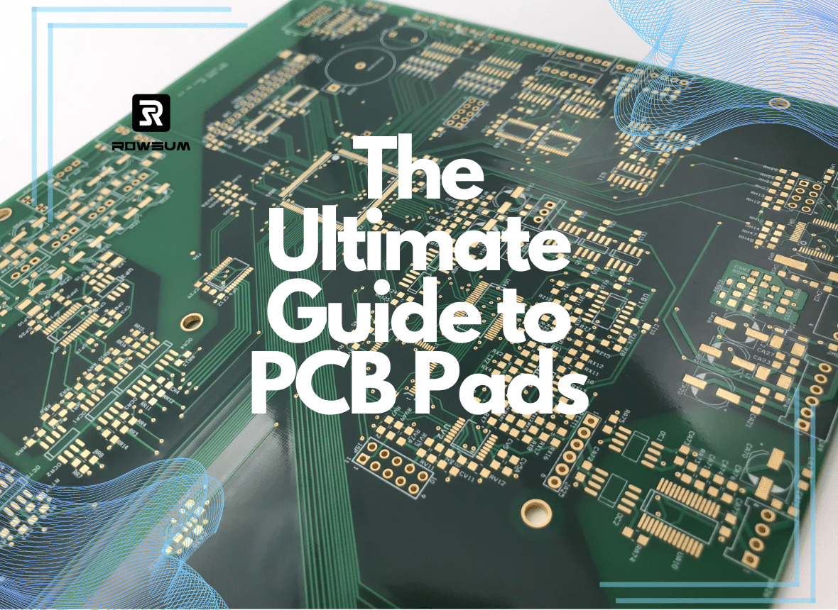
Introduction
Imagine constructing an intricate Lego masterpiece without the small connectors that hold each piece in place. Frustrating, right? Now, picture these connectors failing at a crucial moment. In electronics, PCB pads are akin to those vital connectors. Ensuring their reliability is paramount. But what happens when PCB pads fail?
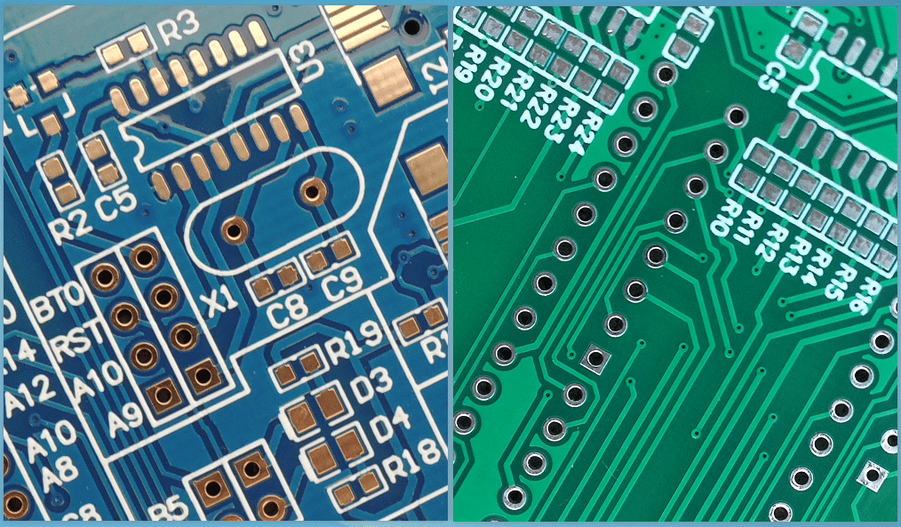
PCB pads, the small conductive areas on printed circuit boards (PCBs), are where electronic components are soldered. They play a critical role in establishing reliable electrical connections and providing mechanical support. Without properly designed PCB pads, electronic devices would fail to function correctly.
In today’s fast-paced electronics industry, these small yet crucial components are fundamental to the functionality and reliability of PCBs. PCB pads not only facilitate essential electrical connections but also provide mechanical stability, making them indispensable for electronic device operation. Different types of PCB pads cater to various purposes and applications, each tailored to meet specific design requirements.
Types of PCB Pads
Through-Hole Pads
Description and Features
Through-hole pads are designed for components with leads that penetrate through the printed circuit board (PCB). These pads are generally larger than their surface-mount counterparts, providing a robust mechanical bond. This makes them particularly suited for components subject to mechanical stress.
Applications and Benefits
Through-hole pads are frequently utilized in scenarios where durability and reliability are paramount, such as industrial equipment and automotive electronics. They offer strong, dependable connections and are easier to inspect and repair compared to surface-mount pads. However, the larger size of through-hole pads means they occupy more space, which can be a limitation in high-density PCB designs.
Surface Mount Pads
Variants: Single-sided and Double-sided
Surface mount device (SMD) pads are designed for components that are mounted directly onto the surface of the PCB. They come in 2 main variants:
- Single-sided: Pads are located on only one side of the PCB.
- Double-sided: Pads are present on both sides of the PCB, allowing for more complex and compact designs.
| Variant | Description | Applications | Benefits | Drawbacks |
|---|---|---|---|---|
| Single-sided | Pads on one side of the PCB | Basic SMD applications | Simpler design, easier to manufacture | Limited to one side, less compact |
| Double-sided | Pads on both sides of the PCB | Complex, high-density designs | Allows for more components, maximizes space | More complex design and manufacturing, harder to inspect |
Applications and Benefits
SMD pads are ubiquitous in modern electronics, primarily due to their support for high-density designs. They facilitate the creation of smaller and lighter devices, making them ideal for consumer electronics such as smartphones and laptops. Despite their benefits, SMD pads necessitate precise manufacturing techniques and can be more difficult to inspect and repair.
Thermal Pads
Description and Importance
Thermal pads are specialized components designed to dissipate heat from electronic parts, ensuring they function within safe temperature limits. These pads typically connect to larger copper areas or heat sinks, facilitating efficient heat transfer away from the components.
Applications and Benefits
Thermal pads are essential in high-power applications, such as power supplies and LED lighting, where overheating can cause failures. By effectively managing heat, thermal pads help extend the lifespan of electronic components and maintain their performance.
Anti-Pads
Description and Role
Anti-pads are specific areas on a printed circuit board (PCB) where copper is intentionally removed to avoid unwanted electrical connections. They are commonly used around vias and other conductive regions to enhance signal integrity.
Applications and Benefits
Anti-pads are crucial in high-frequency and high-speed circuit designs, such as those used in telecommunications and data processing. They help reduce noise and crosstalk, ensuring clean and reliable signal transmission.
Other Specialized Pads
Description and Role
Several specialized pads are used in PCB design, each tailored for specific functions to enhance the functionality and manufacturability of the board. These include castellated holes, test pads, and fiducial markers.
Applications and Benefits
- Castellated Holes: These are plated half-holes along the edge of a PCB, used for edge connectors and modular interfaces. They enable easy soldering of boards to one another, creating stackable or interconnected modules.
- Test Pads: These are small, exposed copper areas on the PCB that provide convenient points for testing and debugging during manufacturing. They facilitate electrical testing and ensure that the PCB functions correctly before final assembly.
- Fiducial Markers: These are precise markers on the PCB used for aligning components during automated assembly. They serve as reference points for pick-and-place machines, ensuring accurate placement of components.
Each of these specialized pads plays a critical role in ensuring the functionality and manufacturability of PCBs, addressing specific design challenges and requirements.
| Type of PCB Pad | Description | Features | Common Applications | Benefits | Drawbacks |
|---|---|---|---|---|---|
| Through-Hole Pads | Pads for components with leads passing through the PCB | Larger, strong mechanical bond | Industrial equipment, automotive electronics | Robust connections, easy inspection and repair | Occupy more space, not suitable for high-density designs |
| Surface Mount Pads | Pads for components mounted directly onto the PCB surface | Single-sided, Double-sided | Consumer electronics, compact designs | Support high-density designs, enable smaller devices | Require precise manufacturing, challenging inspection and repair |
| Thermal Pads | Pads designed to dissipate heat from components | Connect to larger copper areas or heat sinks | High-power applications, LED lighting | Manage heat effectively, extend component lifespan | Can complicate PCB design, require careful placement |
| Anti-Pads | Areas without copper to prevent unwanted connections | Improve signal integrity | High-frequency, high-speed circuits | Reduce noise and crosstalk, ensure clean signals | None significant, specific to certain designs |
| Specialized Pads | Tailored for specific functions (e.g., castellated holes, test pads) | Varies by function | Edge connectors, testing, assembly alignment | Address specific design challenges, ensure manufacturability | Function-specific limitations |
Design Considerations and Practical Tips for PCB Pads
Pad Size and Shape
- Importance in Supporting Components: The size and shape of PCB pads are critical for ensuring robust support for electronic components. Pads that are too small can lead to weak solder joints, while overly large pads can result in solder bridging and other issues.
- Guidelines for Optimal Design:
- Component Specifications: Ensure pad dimensions align with the specifications of the component leads or terminals.
- Standard Guidelines: Adhere to industry standards such as IPC-7351 for SMD pads and IPC-2221 for through-hole pads.
- Pad Geometry: Use rounded or teardrop shapes to reduce stress concentration and improve solder flow.
Spacing and Layout
- Avoiding Short Circuits: Proper spacing between pads is essential to prevent electrical shorts. Inadequate spacing can lead to solder bridges, causing short circuits and potential device failure.
- Ensuring Ease of Soldering:
- Pad Pitch: Maintain a consistent pitch between pads to facilitate automated soldering processes.
- Solder Mask Clearance: Ensure there is enough clearance between the pad and the solder mask to avoid unwanted solder flow.
Material Selection
- Durability and Electrical Reliability: The materials used for PCB pads must provide durability and excellent electrical conductivity. The choice of material significantly impacts the pad’s performance and longevity.
- Common Materials Used:
- Copper: The most commonly used material due to its excellent electrical conductivity.
- Surface Finishes: Apply finishes such as HASL (Hot Air Solder Leveling), ENIG (Electroless Nickel Immersion Gold), or OSP (Organic Solderability Preservatives) to enhance solderability and protect against oxidation.
Conclusion
In the dynamic world of electronics, PCB pads are crucial connectors that ensure seamless operation. These small yet essential components provide stable electrical connections and mechanical support to your devices. Getting them right is vital for your devices’ reliability and performance.
By understanding the different types of PCB pads and their applications, you can make informed decisions that enhance your PCB designs. Whether it’s through-hole, surface mount, thermal, or specialized pads, each type has its role in creating a robust and functional board.
Remember, the devil is in the details. Following industry standards, choosing the right materials, and testing thoroughly are the keys to success. At Rowsum, we’re here to support you every step of the way with high-quality PCB solutions tailored to your needs.
Ready to take your PCB designs to the next level? Contact us today!
Frequently Asked Questions (FAQs)
What are pads in PCBs?
Pads in PCBs are small conductive areas where electronic components are soldered. They create electrical connections and provide mechanical support for the components.
Can you replace a pad on PCB?
Yes, you can replace a pad on a PCB. This process typically involves removing the damaged pad, cleaning the area, and applying a new pad using a repair kit or conductive epoxy.
Can a PCB be repaired?
Yes, a PCB can be repaired. Common repairs include fixing broken traces, replacing damaged pads, and resoldering loose components. Professional repair services can handle more complex issues.
What are pads vs vias in PCB?
Pads are conductive areas where components are soldered, while vias are holes that allow electrical connections between different layers of a PCB. Pads support component placement, whereas vias facilitate interlayer connections.
What is the standard pad size for PCB?
The standard pad size for a PCB varies based on the component and the type of pad. For through-hole components, pad sizes typically range from 1.5 to 2 times the lead diameter. For surface mount components, pad sizes follow industry standards such as IPC-7351, which provide specific dimensions based on the component’s package type.